Parallel DACs High-quality DIY USB audio adapter Homemade hi-fi level DAC
Most parallel DAC circuits are based on the summation of currents, the strength of each of which is proportional to the weight of the digital binary bit, and only the bit currents whose value is equal to 1 should be summed. For example, suppose you want to convert a four-bit binary code into an analog current signal. The fourth, most significant digit (MSB) will have a weight of 2 3 =8, the third digit will have 2 2 =4, the second will have 2 1 =2, and the least significant digit will have 2 0 =1. If the weight of the MZR I MZR =1 mA, then I SZR =8 mA, and the maximum output current of the converter I output max = 15 mA and corresponds to code 1111 2. It is clear that the code 1001 2, for example, will correspond to I out =9 mA, etc. Consequently, it is necessary to construct a circuit that ensures generation and switching of precise weighing currents according to given laws. The simplest circuit that implements this principle is shown in Fig. 3.
The resistance of the resistors is chosen so that when the switches are closed, a current corresponding to the weight of the discharge flows through them. The key must be closed when the corresponding bit of the input word is equal to one. The output current is determined by the relation

With a high bit capacity of the DAC, the current-setting resistors must be matched with high accuracy. The most stringent accuracy requirements are imposed on resistors of the highest digits, since the spread of currents in them should not exceed the current of the low-order digit. Therefore, the resistance spread in k-th digit must be less than
D R /R=2 –k
From this condition it follows that the spread of the resistor resistance, for example, in the fourth digit should not exceed 3%, and in the 10th digit – 0.05%, etc.
The considered scheme, for all its simplicity, has a whole bunch of disadvantages. Firstly, for different input codes, the current consumed from the reference voltage source (RPS) will be different, and this will affect the value of the output voltage RES. Secondly, the resistance values of weight resistors can differ by thousands of times, and this makes it very difficult to implement these resistors in semiconductor ICs. In addition, the resistance of the high-order resistors in multi-bit DACs can be comparable to the resistance of the closed switch, and this will lead to a conversion error. Thirdly, in this circuit, significant voltage is applied to the open switches, which complicates their construction.
These shortcomings were eliminated in the AD7520 DAC circuit (domestic analogue of 572PA1), developed by Analog Devices in 1973, which is now essentially an industry standard (many serial DAC models are made according to it). The indicated diagram is shown in Fig. 4. MOS transistors are used here as switches.

Rice. 4. DAC circuit with switches and constant impedance matrix
In this circuit, the setting of the weighting coefficients of the converter stages is carried out by sequentially dividing the reference voltage using a resistive matrix of constant impedance. The main element of such a matrix is a voltage divider (Fig. 5), which must satisfy the following condition: if it is loaded with resistance R n, then its input impedance R inx must also take the value R n. Chain attenuation coefficient a = U 2 /U 1 at this load must have the specified value. When these conditions are met, we obtain the following expressions for resistances:
in accordance with Fig. 4.
Since in any position of the switches S k they connect the lower terminals of the resistors to the common circuit bus, the reference voltage source is loaded with a constant input impedance R in = R. This ensures that the reference voltage remains unchanged for any DAC input code.
According to Fig. 4, the output currents of the circuit are determined by the relations
| (8) |
| (9) |
and the input current
| (10) |
Since the lower terminals of the resistors 2 R matrices for any switch state S k connected to the common circuit bus through the low resistance of the closed switches, the voltages on the switches are always small, within a few millivolts. This simplifies the construction of switches and control circuits and allows the use of reference voltages from a wide range, including different polarities. Since the DAC output current depends on U op linear (see (8)), converters of this type can be used to multiply an analog signal (applying it to the reference voltage input) by a digital code. Such DACs are called multiplying(MDAC).
The accuracy of this circuit is reduced by the fact that for high-bit DACs, it is necessary to match the resistance R 0 switches with discharge currents. This is especially important for high-order keys. For example, in the 10-bit AD7520 DAC, the key MOSFETs of the six most significant bits are made different in area and their resistance R 0 increases according to the binary code (20, 40, 80, ..., 640 Ohm). In this way, the voltage drops across the switches of the first six bits are equalized (up to 10 mV), which ensures monotonicity and linearity of the DAC transient response. The 12-bit DAC 572PA2 has a differential nonlinearity of up to 0.025% (1 LSB).
DACs based on MOS switches have relatively low performance due to the large input capacitance of the MOS switches. The same 572PA2 has a settling time of the output current when changing the input code from 000...0 to 111...1, equal to 15 μs. The Burr-Braun 12-bit DAC7611 has an output voltage settling time of 10 µs. At the same time, DACs based on MOS switches have minimal power consumption. The same DAC7611 consumes only 2.5 mW. Recently, DAC models of the type discussed above have appeared with higher performance. Thus, the 12-bit AD7943 has a current settling time of 0.6 μs and a power consumption of only 25 μW. Low self-consumption allows such micro-power DACs to be powered directly from the reference voltage source. Moreover, they may not even have a pin for connecting an ION, for example, AD5321.
DAC on current sources
DACs based on current sources have higher accuracy. Unlike the previous version, in which the weight currents are formed by resistors of relatively low resistance and, as a result, depend on the resistance of the switches and the load, in this case the weight currents are provided by transistor current sources with high dynamic resistance. A simplified circuit of a DAC using current sources is shown in Fig. 6.

Rice. 6. DAC circuit on current sources
The weight currents are generated using a resistive matrix. The potentials of the bases of the transistors are the same, and in order for the potentials of the emitters of all transistors to be equal, the areas of their emitters are made different in accordance with the weighting coefficients. The right resistor of the matrix is not connected to the common bus, as in the diagram in Fig. 4, and to two identical transistors connected in parallel VT 0 and VT n, as a result of which the current through VT 0 is equal to half the current through VT 1 . The input voltage for the resistive array is generated using a reference transistor VT op and operational amplifier OU1, the output voltage of which is set such that the collector current of the transistor VT op takes value I op. Output current for N-bit DAC.
| (11) |
Typical examples of DACs based on current switches with bipolar transistors as switches are the 12-bit 594PA1 with a settling time of 3.5 μs and a linearity error of no more than 0.012% and the 12-bit AD565, which has a settling time of 0.2 μs with the same linearity error. The AD668 has even higher performance, with a settling time of 90 ns and the same linearity error. Among the new developments, we can note the 14-bit AD9764 with a settling time of 35 ns and a linearity error of no more than 0.01%.
As current switches S k bipolar are often used differential stages, in which the transistors operate in active mode. This allows the settling time to be reduced to a few nanoseconds. The current switch circuit for differential amplifiers is shown in Fig. 7.

Differential cascades VT 1 –VT 3 and VT" 1 –VT" 3 are formed from standard ESL valves. Current Ik, flowing through the collector terminal of the output emitter follower is the output current of the cell. If to digital input Dk When a high level voltage is applied, transistor VT 3 opens and transistor VT" 3 closes. The output current is determined by the expression

Accuracy is greatly improved if the resistor R e replace with a direct current source, as in the circuit in Fig. 6. Due to the symmetry of the circuit, it is possible to generate two output currents - direct and inverse. The fastest models of such DACs have ESL input levels. An example is the 12-bit MAX555, which has a settling time of 4 ns to the 0.1% level. Since the output signals of such DACs cover the radio frequency range, they have an output impedance of 50 or 75 ohms, which must be matched to the characteristic impedance of the cable connected to the output of the converter.
Formation of the output signal in the form of voltage
There are several ways to generate the output voltage for a DAC with summation of weight currents. Two of them are shown in Fig. 8.

Rice. 8. Formation of voltage using the current output of the DAC
In Fig. Figure 8a shows a circuit with a current-to-voltage converter on an operational amplifier (op-amp). This circuit is suitable for all current output DACs. Since the film resistors that determine the weight currents of the DAC have a significant temperature coefficient of resistance, the feedback resistor R The os should be made on the DAC chip and in the same technological process, which is usually done. This makes it possible to reduce the temperature instability of the converter by 300...400 times.
For a DAC based on MOS switches, taking into account (8), the output voltage of the circuit in Fig. 8a.
![]()
Typically the resistance of the feedback resistor is R os = R. In this case
| (12) |
Most DAC models have significant output capacitance. For example, for AD7520 with MOS switches, depending on the input code WITH output is 30...120 pF, for AD565A with current sources WITH out = 25 pF. This capacitance together with the DAC output resistance and resistor R OS creates an additional pole in the frequency response of the op-amp feedback loop, which can cause instability in the form of self-excitation. This is especially dangerous for DACs with MOS switches with a zero input code. At R os =10 kOhm, the frequency of the second pole will be about 100 kHz at 100% feedback depth. In this case, an amplifier whose unity gain frequency f t exceeds 500 kHz, will have clearly insufficient stability margins. To maintain stability, you can connect it in parallel with a resistor R OS capacitor WITH k, the capacity of which, to a first approximation, can be taken equal to WITH exit For a more accurate selection WITH It is necessary to conduct a full analysis of the stability of the circuit, taking into account the properties of a specific op-amp. These measures degrade the performance of the circuit so seriously that a paradoxical situation arises: to maintain high performance of even an inexpensive DAC, a relatively expensive high-speed (short settling time) op-amp may be required.
Early DAC models with MOS switches (AD7520, 572PA1, etc.) allow a negative voltage on the switches of no more than 0.7 V, therefore, to protect the switches, a Schottky diode should be included between the DAC outputs, as shown in Fig. 8a.
For a digital-to-analog converter on current sources, the conversion of the output current into voltage can be done using a resistor (Fig. 8b). In this circuit, self-excitation is impossible and the speed is maintained, however, the amplitude of the output voltage should be small (for example, for AD565A in bipolar mode within ± 1 V). Otherwise, the current source transistors may go out of linear mode. This mode is provided at low load resistance values: R n » 1 kOhm. To increase the amplitude of the DAC output signal in this circuit, you can connect a non-inverting op-amp amplifier to its output.
For DACs with MOS switches, in order to obtain an output signal in the form of a voltage, you can use the inverse connection of the resistive matrix (Fig. 9).

Rice. 9. Inverse connection of DAC with MOS switches
To calculate the output voltage, we find the relationship between the voltage U i on the key S i and nodal voltage U"i. Let's use the principle of superposition. We will consider all voltages on the switches equal to zero, except for the voltage under consideration U i. At R n =2 R Loads with resistance 2 are connected to each node on the right and left R. Using the two-node method, we get

We will find the output voltage of the DAC as the total voltage at the rightmost node, caused by the total action of all U i. In this case, the voltages of the nodes are summed with weights corresponding to the division coefficients of the resistive matrix R- 2R. We get
![]()
To determine the output voltage at an arbitrary load, we use the equivalent generator theorem. From the equivalent DAC circuit in Fig. 10 it is clear that

Generator equivalent resistance R e coincides with the input resistance of the matrix R- 2R, i.e. R e = R. At R n =2 R from (14) we get
The disadvantages of this circuit are: a large voltage drop across the switches, a varying load of the reference voltage source and significant output resistance. Due to the first drawback, this scheme cannot include DACs of type 572PA1 or 572PA2, but 572PA6 and 572PA7 can be used. Due to the second drawback, the reference voltage source must have a low output impedance, otherwise the conversion characteristic may be non-monotonic. However, the inverse connection of a resistive matrix is quite widely used in DAC ICs with a voltage output, for example, in the 12-bit MAX531, which also includes a built-in op-amp in a non-inverting connection as a buffer, or in the 16-bit MAX542 without a built-in buffer . The AD7390 12-bit DAC is built on an inverse matrix with an on-chip buffer amplifier and consumes only 0.3 mW of power. True, its settling time reaches 70 μs.
Parallel switched capacitor DAC
The basis of this type of DAC is a matrix of capacitors, the capacitances of which are related as integer powers of two. A diagram of a simple version of such a converter is shown in Fig. 11. Capacity k th matrix capacitor is determined by the relation
The capacitor also receives an equal charge WITH in op-amp feedback. In this case, the output voltage of the op-amp will be
To store the conversion result (constant voltage) for any length of time, a sample-and-hold device should be connected to the output of this type of DAC. Converters based on switched capacitors cannot store the output voltage for an unlimited time, as DACs with summation of weight currents and equipped with a latch register can do, due to charge leakage. Therefore, they are used mainly as part of analog-to-digital converters. Another disadvantage is the large area of the IC chip occupied by such a circuit.
DAC with voltage summation
The circuit of an eight-bit converter with voltage summation, manufactured in the form of an IC, is shown in Fig. 8.12. The converter is based on a circuit of 256 resistors of equal resistance connected in series. Conclusion W through the keys S 0 …S The 255 can connect to any point in this circuit depending on the input number. Input binary code D is converted by the 8x256 decoder into a unitary positional code that directly controls the keys. If you apply voltage U AB between pins A And IN, then the voltage between the terminals W And B will be
U WB = U AB D.
The advantage of this scheme is low differential nonlinearity and guaranteed monotonicity of the conversion characteristic. It can be used as a digitally adjustable resistor. Several models of such DACs are available. For example, the AD8403 chip contains four eight-bit DACs, designed according to the circuit in Fig. 8.12, with resistance between terminals A And IN 10, 50 or 100 kOhm depending on the modification. When an active level is applied to the “Economic mode” input, the key opens S switch off and close the key S 0 . The IC has a reset input that can be used to set the DAC to the middle of the scale. Dallas Semiconductor produces several DAC models (for example, dual DS1867) with voltage summation, in which the input register is a non-volatile random access memory device, which is especially convenient for building circuits with automatic adjustment (calibration). The disadvantage of the circuit is the need to manufacture on a chip a large number of(2 N) matched resistors. However, 8, 10 and 12-bit DACs of this type with output buffer amplifiers are currently available, for example, AD5301, AD5311 and AD5321.
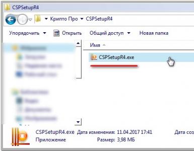
Being the “lucky” owner of an integrated sound subsystem, I still dreamed of a good sound card, and could not even think that I could make it myself at home. One day, while surfing the World Wide Web, I came across a description of a sound card with a USB interface on a PCM2702 chip from Burr-Brown and, having looked at the price lists of companies selling radio components, I realized that this was not for us yet - no one knew anything about it. Later, my computer was built in a small microATX case, which did not have enough space even for the old Creative Audigy2 ZS. I had to look for something small and preferably external with a USB interface. And then again I came across the PCM2702 chip, which was already actively used and praised for the quality of music playback - with the right circuit design, the sound was much more pleasant than that of the same Audigy2 ZS. Search again by price lists, and lo and behold, the required microcircuit is available at a price of about 18 “enemy money”. As a result, a couple of chips were ordered for experiments, so to speak, to listen to what the bourgeois “DAC builders” had put together.
So, what kind of beast is this PCM2702 controller, from the legendary Burr-Brown company, which has won the hearts of audiophiles all over the world with its top solutions? Wondering what a budget solution can do?
According to the technical documentation for the chip (pcm2702.pdf), we have a digital-to-analog converter (DAC) with a USB interface with the following characteristics:
- Bit size 16 bits;
- Sampling rates 32 kHz, 44.1 kHz and 48 kHz;
- Dynamic range 100 dB;
- Signal-to-noise ratio 105 dB;
- Nonlinear distortion level 0.002%;
- USB1.1 interface;
- Digital filter with 8x oversampling;
- Works with standard USB audio device driver.
Now about the device itself. To begin with, a simple version was assembled according to the manufacturer’s recommended scheme with minor changes in nutrition. The result was a small “sound speaker” powered by USB.

But such a device was not complete and required an external amplifier, and it could not drive the headphones properly. Was later replaced motherboard to another, with a normal HAD codec and good board layout. The audio path was devoid of extraneous noise and rustling, and the quality of the output signal was no worse than that of the PCM2702. And, probably, these lines would not have existed, if only such a box had not caught my eye:


This is a passive cooling system for HDD, but for me, first of all, it is a chic case for radio equipment. I immediately realized that it would contain something, for example, a sound card with an amplifier; fortunately, there should be no problems with cooling. I thought a lot about the circuit design of the device. On the one hand I wanted High Quality, and on the other hand, I didn’t want to pay more than ready-made sound cards from Creative cost. The main question arose regarding the LPF and headphone amplifier, because high-quality components for these purposes can cost as much as the PCM2702 itself, or even more. For example, the price of high-quality operational amplifiers for LPF - OPA2132 and OPA627, cost about 10 and 35 dollars, respectively. I didn’t find any headphone amplifier chips - AD815 or TPA6120 in the price lists, and the prices for them are also not small.
But there is always a silver lining, and I found on the Internet a circuit of a simple and high-quality LPF on transistors, the author of which claimed decent sound, even no worse than expensive operational amplifiers. I decided to try it. As a headphone amplifier I installed the LM1876 chip - the younger two-channel “sister” of the legendary LM3886 with the same sound but less power. This microcircuit allows you to connect speakers by increasing the gain.
The result is this diagram - USB-DAC_PCM2702_Sch.pdf, drawing printed circuit board- USB-DAC_PCM2702_Pcb.pdf in mirror image for transferring an image using the laser-iron method onto copper foil, the so-called LUT (you can read more on the Internet), a drawing of the arrangement of elements and jumpers on the board, as well as a diagram for connecting the volume control - USB-DAC_PCM2702. pdf.
When assembled, the board looks like this:


I’ll tell you a little about how it all works, if suddenly there are people who want to assemble such a unit. The PCM2702 connection circuit is standard - the LPF is a Sallen-Kay filter, a second-order low-pass filter with unity gain, since the active element works as a follower, you can use an emitter or source follower without any problems. There is already room for experimentation here. You can choose the type of transistors that you like best in terms of sound - testing from what was available, I settled on the KT3102E in a metal case (VT3, VT4 - see diagram USB-DAC_PCM2702_Sch). The filter elements most affect the sound, especially capacitors C25, C26, C31, C32. Experts in this matter recommend installing WIMA FKP2 film capacitors, FSC foil polystyrene or Soviet PM. But there was nothing normal in stock and I had to install what I had, and only then I exchanged it for a better one. The board has contact pads for both output and SMD capacitors. Resistors R9, R10, R11, R12 are needed in pairs identical, for which we take resistors with an accuracy of 1% or select pairs using a multimeter. I selected from several dozen resistors with an accuracy of 5%, since there was no time to wait until they brought them with an accuracy of 1%. The values of resistors and capacitors can be selected according to the sound, as you like best, but the only condition is that the pair must be the same so that each channel does not sing differently.
The circuit provides for disconnecting the PCM2702 analog power supply and the filter output from connectors X5, X6 if the USB cable is not connected to connector X1. This is done so that the low output impedance of the filter does not interfere with the signal supplied to these connectors when using the device as a headphone amplifier. When connected, the analog power to the DAC is supplied through transistor VT2, which is controlled by transistor VT1; if there is voltage at the USB connector, then both transistors are open. The filter outputs are connected to the connectors on the rear panel via relay K1, which is also controlled by power from USB. I used the relay V23079-A1001-B301 from AXICOM. If there is no such relay, then instead of it you can install a regular switch with two contact groups. Instead of transistor VT2, you can also install a switch, and all the elements responsible for switching the power supply will not need to be soldered in, but it is advisable to switch the USB power supply itself through the same switch.
The amplifier and analog part are powered by an external power source with a voltage of 12-15 V and 0.5 A AC, connected via connector X2 on the rear panel.

The power supply itself was made from a conventional stabilized 12 V 0.5 A power supply by throwing away everything unnecessary.

In the amplifier, you also need to select resistors R15-R18 in pairs, which set the gain (left channel Cool = R17/R15, Coup = R18/R16). If you do not plan to use headphones, then you can connect speakers, then you need to reduce the resistance of resistors R15, R16 to 4.7-10 kOhm, you can slightly increase the resistance of R17, R18. Thus, it will be possible to obtain a nominal output power of about 2 x 5 W. If you power the D6 microcircuit with a voltage of +/- 20...25 V, which is taken immediately after the rectifier from capacitors C6, C7, you can get a maximum output power of 2 x 18 W, but for this you will need to install diodes VD2, VD3 with a current of at least 3A , replace fuse F2 with a current of at least 3A, double the capacity of condensates C6, C7 and use a transformer in a power supply of higher power, approximately 16 V 4 A AC.
All SMD resistors, resistors R20, R22 with standard size 1206, resistors R13, R14 with standard size 2010, jumpers can be installed instead of them, all other resistors with standard size 0805. All SMD ceramic capacitors with standard size 0805, all electrolytic capacitors with a maximum operating temperature of 105 ° C and low internal resistance , with an operating voltage of 16 V, capacitors C6, C7 with a maximum operating voltage of 25-35 V. Most of the connectors are soldered from old equipment, I can’t say the exact markings, refer to appearance. The volume control resistor is connected with a two-core shielded wire, two signal channels and ground across the screen, a resistor of unknown Chinese origin with a resistance of 20 kOhm group B (with an exponential dependence of the resistance on the angle of rotation of the knob).
I also want to tell you a little about how to solder microcircuits in such a small case. Some people mistakenly believe that such microcircuits need to be soldered with low-power soldering irons and a thin tip. It's very funny to watch when people sharpen the tip like an awl and try to solder each leg separately with it. In fact, everything is easy and simple. First, install the microcircuit in the desired position, hold it with your hand or fix it with glue, solder one of the outer terminals, then center it, if necessary, and solder the opposite terminal. If several pins are soldered together, then this is not a problem. Use a soldering iron with a power of 30-50 W with a tinned, freshly sharpened tip at an angle of about 45°, and do not skimp on flux or rosin. The flux should preferably not be active, otherwise you will have to wash the board very carefully trying to wash it out from under the microcircuit. We warm up all the legs with a small drop of solder, starting from one edge and gradually, as it warms up, we move the soldering iron towards the unsoldered leads, driving off excess solder onto them, while the board can be held at an angle so that the solder itself flows down under the influence of gravity. If there is not enough solder, take another drop; if there is a lot, then using a rag we remove all the solder that is on the soldering iron tip, and without sparing the flux, we remove the excess from the terminals of the microcircuit. Thus, if the board is properly etched, well cleaned and degreased, then soldering takes place within 1-3 minutes and turns out clean, beautiful and uniform, as can be seen on my board. But for greater confidence, I recommend practicing on burnt boards from different computer equipment with microcircuits that have approximately the same pin pitch.
I recommend that you do not first solder in the D2 and D6 microcircuits and elements that may interfere with their installation. First of all, it is necessary to solder the nodes responsible for power supply, test the power circuit for short circuits, connect it to the USB port and supply 14 V alternating voltage from the power supply to X2. Future outputs of stabilizer chips should have the following voltages:
- D1: +3.3 V;
- D3: +12 V;
- D4: -12 V;
- D5: +5 V.
When you connect the PCM2702 to your computer for the first time, the system finds a new device - Burr-Brown Japan PCM2702 USB Speakers.

After the driver is automatically installed in Device Manager, a new device will appear - USB Speakers. This means that everything works, since you can and should turn on music, videos, or even run games.

The system automatically transfers sound to the PCM2702 chip when it is connected to a computer and returns it to its original state when the board is disconnected; to resume playback, you just need to restart the desired program. Volume is adjusted using the standard Windows volume control. I checked the performance of the board only under Windows system XP SP2.
A little about assembling the entire device into a housing. The most difficult thing is installing a variable resistor for the volume control. The front panel is attached to the chassis via a protrusion that runs along the back side of the panel and is quite thick. This protrusion needs to be cut off with a hacksaw or a milling machine in the place where the volume control will be attached, but you need to be very careful, as you can scratch the aluminum coating, which will cause the panel to lose its attractiveness. Then we drill a hole for attaching the resistor, the location for which is estimated based on the position of the handle that will be put on this same resistor. WITH front side We remove the ribs near the hole a little so that the nut reaches the threads on the base of the resistor. There is one more problem - the center of the panel does not coincide with the center of the internal chamber of the chassis, and the volume control resistor rests against the body. I had to raise the panel by 2-3 mm, for which I cut off the corner of the protrusion for fastening with a Dremel.
I will not describe in detail all the actions with the panel and chassis. Those who can make this kind of device themselves will understand everything from the photographs. Where holes needed to be drilled and threads cut, during installation 2 washers were placed under the panel near each screw to raise it by 2 mm. The chassis also has holes drilled and threaded for mounting the board. Chips D3, D4 and D6 are pressed to the chassis with M2.5 screws, while D4 and D6 need to be isolated from the panel using a mica plate or other heat-conducting dielectric or use chips with an insulated housing, like D6 in my case. Back panel made from a plastic plug from the system unit. All this can be seen in more detail in the photo.
Here electrical diagram a homemade digital-to-analog converter that uses the PCM2707 chip - a ready-made USB DAC module. It is defined as a USB Audio Class 1.0 device and does not require any special drivers.
The circuit is made according to the datasheet, only a couple of indicator LEDs have been added so that it can be seen when the device is turned off and connected to the computer. We also installed a choke on the USB 5V line to suppress any high-frequency noise that could theoretically leak through the DAC power supply.

When installing a DAC, try to use surface-mounted radio components. Most passive components (resistors, capacitors, ferrite beads) are size 0805.

On the PCM2707 chip, it is possible to use the volume, play, pause and skip buttons for the song on the computer to which the unit is connected. IN this option There are no plans to use these functions, but the contact pins have been added in case we use something in the future.


And this is a view of the assembled USB DAC decoder PCB, which immediately worked the first time it was connected. In this case, headphones are used to listen to music, but you can connect any homemade amplifier.

Hi all. Today I want to talk about a fairly good entry-level USB DAC.
This device The following categories of people should be interested:
1) Users of laptops and stationary devices with a faulty built-in audio card.
2) Users of laptops whose manufacturer has not fully added support for Windows 10.
This is exactly my case, more details:
Expand explanation
At work they gave me a “new” used laptop to replace my Lenovo T420, which ran on Windows 7 and was in very good condition, but not compatible with Windows 10, which the company decided to switch to completely, for a number of reasons (officially due to security, but it is clear that the support and compatibility factor also played a role here, not only from Microsoft).
They gave me an HP Revolve 810, which seems to be compatible with Windows 10. Everything seems to be there, but there is no official driver specifically for the sound system! Since the audio is quite rare, IDT:
HDAUDIO\FUNC_01&VEN_111D&DEV_76E0&SUBSYS_103C21B3&REV_1003
(Intel also liked to install such chips on its motherboards), there is nowhere to find firewood.
On the HP forum I came across a link to a compatible driver from the same user as me, and he says that the driver is crooked...
Since the driver was taken from an unknown place, and it is not yet clear how well it works, I decided not to install it on my work laptop, and I had to be content with a standard Windows driver.
As practice has shown, you can use a standard, automatically installed driver for audio, but the sound will be worse than it could have been with the driver.
If you have a desktop board, then when using such a driver, problems may arise with the functionality of the line input, as well as with other functions. In addition, when working on a “standard” driver, there is no equalizer, which, among other things, can be adjusted, for example, when using foobar2000.
After Lenovo T420, on the same headphones, the sound did not suit me. Yes, it seems to play, and it seems to be without distortion, but I don’t really want to listen to the music because it is presented somehow dryly, without the same emotional coloring or something.
3) As an alternative audio card on portable devices running Android (I conventionally call it an audio card, since the subject does not have a microphone input, which is usual for this category of devices). I can’t say about IOS, maybe it will work there too.
4) Users of other devices that do not have audio on board, and which have a compatible OS.
Earlier, similar devices were already reviewed on this site, but I couldn’t find them in this design after looking among those previously reviewed.
I’ll immediately note that there is a more affordable analogue of this DAC:
, the cost is about 2 times lower, but the workmanship and materials are worse... I was thinking about buying it for comparison, but I haven’t done it yet, since in any case I will redo the output (and this is extra time), and I haven’t played enough with the first DAC yet -ohm.
On Aliexpress, by the way, DACs based on PCM2704 are 2 times more expensive, and there are mainly “large” options there, those with optical output and RCA.
Let's move on to the DAC we are reviewing
The board is made of very high quality. The textolite is very thick, the soldering is quite neat, the flux has been washed off. The scarf looks very nice, but it would still be better if it were in a case. The manufacturer was not greedy and installed tantalum capacitors in the output filter. See for yourself:


Operation and impressions of work.
Getting started with a DAC is very easy. Manual installation of any drivers is not required. Under Windows XP/7/10, the driver was picked up automatically.

Unlike the built-in audio, the DAC plays noticeably louder at the same volume level. It plays quite well, a little better than the audio built into my laptop, but the difference is not particularly noticeable, at the level of error.
According to a colleague, with a Lenovo laptop, which was lucky with the presence of realtek (and, accordingly, full-fledged firewood for ten), his laptop has a more interesting built-in than this DAC.
Personally, in my opinion, the subject lacks “meat” (I picked up this rather appropriate allegory on some “audio forum”) and detail, at least when using headphones with an impedance of 32 Ohms.
My headphones are so-so, but not the worst:

This is Pioneer SE-MJ21.
Especially for the tests, additional headphones adapted for portable equipment were purchased at a big discount, including those tailored for equipment from the manufacturer of Apple products:

In these headphones, apparently due to the high sensitivity, the DAC screams even louder, the sound is more pleasant and interesting if you listen to the sound at the same volume as in the previous headphones, but not very loudly.
Apparently this is due to the low power of the amplifier built into the PCM2704C and quite large distortions when operating at a 32 Ohm load. The DAC itself is so-so by audiophile standards, which is confirmed by the parameters from the datasheet.
I don’t currently have a “cooler” DAC to compare them head-on.
I don’t consider myself an audiophile, but still, often their words are not without meaning, even if they disagree with the data from the documentation, but this seems to be a rare event.
As I already noted, the subject is built on PCM2704 C, there is also an older version of the PCM2704 chip, without the “C” prefix, which TI does not recommend for new projects. As far as I understand from a fairly superficial study of the datasheet, there are no particular differences between the chips, the pinouts and characteristics are the same.
Work under Android:
The DAC works under Android, is detected by the phone within 5 seconds and then off we go.
I only did a quick test, trying out a couple of players. All of them reproduce sound through the DAC, but cannot control the volume, so the volume is at maximum.
I still need to delve into the settings, but I can’t do this now, since I tested it briefly, on other people’s smartphones, due to the fact that my red rice “ran out” about two weeks ago, and the Russian Post has been freezing the parcel in Moscow for a week now, it’s hard I can’t wait any longer with the review)). Later, I think I’ll add to the review or publish a separate note for Android, with a note about adjusting the sound.
I haven't tested the functionality under Linux, but it should work. If any of the Muskovites are very interested, I can check it out.
It was evening, there was nothing to do... Customization.
I decided to build a simple amplifier (a test model, nothing more) on the available dual operational amplifiers, intended for audio, what if it “rocks” the exhaust, I thought.
It so happened that I had two such microcircuits, and both were different. One NE5532P bought in a local chip and dip for 15 rubles, and an OPA2134 bought a couple of years ago on taobao, it seems to be real).
When I was assembling the amplifier, I first assembled one channel, and for several days I drove it with different op-amps, quickly moving them from the socket previously provided for these purposes, right during listening. The sound was different, but more on that in another section.
In the “finished project” (I think everything is just beginning, if I’m not too lazy) I use two NE5532AP, from a chip and a dip, they are 21 rubles each).
The result is this “creation”, intended for running and testing: 
There are a lot of long wires here, but this is only in less significant parts of the circuit; the input is made as short as possible (except for the electrolyte) and in the screen.
One of the channels: 
Here the power supply is pulsed, from a powerbank, one of the first implementations. More information about nutrition below.
Amplifier circuitry.
So the existing minijack (culturally made) was lost somewhere at home, it was decided to solder it to the corresponding legs of the chip to receive an input signal to the amplifier.
According to the documentation, legs 14-15 are responsible for outputting the signal from the DAC. I soldered it to these legs using a relatively thin 50 Ohm antenna cable: . At the same time, a thin, varnished copper wire, approximately 0.2 mm thick, was soldered to the leg itself (I don’t have a micrometer, so I can’t say for sure, and it’s not that important) and it was already soldered to the cable core. The cable screen was soldered to the GND of the board, which was found between two ceramic capacitors, identical for each of their channels.
The amplifier itself is based on the following, simple circuit for connecting a dual op-amp as a headphone amplifier, reviewed by BB (TI): 
The diagram is taken from here:
A series chain of a 4.7K resistor and a 10uF electrolytic capacitor was added to the input of this circuit. The capacitor is connected positive to the input signal.
Also, a resistor was added between the non-inverting input of the first op-amp and ground.
Here is the final diagram: 
How I soldered and how I configured it.
A couple of years ago I soldered a preamp for a dynamic microphone, and learned something from it:
Firstly, if a test prototype is being made, including a surface-mounted one, the wire connections should be as short as possible and minimized as much as possible. The distance between components should also be minimal.
Low-current input circuits must be shielded and must not interfere with power supply.
All this will help reduce the input noise of the amplifier.
Initially, I soldered variable resistors to test the input filter and to adjust the gain, despite the fact that it is usually set in advance, and the power is already regulated by a variable resistor located at the input, in front of the filter.
In the final version of the layout, I left only a 4.7K variable connected in series with a 3.3K resistor, for each channel, which sets the gain in the circuit.
In addition, I had to tinker with the input filter in search of optimal parameters. Here I looked at the diagram of this unit:
I found about a dozen different capacitors in my supplies. These were paper, electrolytes, film and others:
Capacitors

As a result, I liked the sound of the 63V 10uF electrolyte, in front of which a 4.7K resistor was placed.
About nutrition
In this circuit, the op-amp must be powered from a bipolar power source.
A converter from one polar voltage to two polar was needed.
From Ebay, now somewhere there is a specialized microcircuit for these purposes, but it was taken simply to compare the difference with a relatively normal bipolar power supply (which I planned to assemble myself), since Kirich successfully tested it on this site and found that it was “noisy”, which is not good for audio. When it arrives, I'll check it and report back.
As a result, this scheme was taken as a basis: